Embedded Firmware Development For A Resource-Constrained System

So, you want to make the world's smallest and most power-efficient wireless sensors. How do you make the firmware for that?
The Challenge
The wireless sensors from Disruptive Technologies are powered by tiny coin cell batteries. These batteries offer long life in terms of low self-leakage but don't really pack a punch in terms of total energy. (Brief aside: This is actually a benefit in some cases, for instance when operating in potentially explosive atmospheres).
To put the challenge in numbers: The Varta CR1216 coin cell datasheet claims 27 mAh capacity and a self-discharge rate < 1% / year at room temperature. (Compare this to AA batteries that typically have 2000 to 3000 mAh capacity.)
So for a sensor to last 15 years on a CR1216 battery, it should not draw more than a total of around 23 mAh (27 mAh minus potential self-discharge) over the whole 15 years. This means that the average current must be less than 175 nA! This average must include the current spent on sensing, wireless communication, and static leakage.
In comparison, just the standby current of most wireless MCUs is much higher than this, even when doing nothing else than keep a timer running and (some of) the RAM content alive. For example, the CC1350 from Texas Instruments lists 700 nA as the typical current in the lowest available standby mode with a low-power clock running and full RAM retention. The EFR32FG14 from Silicon Labs claims 550 nA with a low-power clock running and 128 byte RAM retention. Even though these are very competitive numbers, we are clearly not able to reach our goals based on this alone.
The Disruptive Technologies Solution
To overcome the challenge, the sensors from Disruptive Technologies include an ASIC that has been designed with an extreme focus on low power consumption.
This ASIC is responsible for time-keeping, capacitive sensing (for touch and proximity), external sensor read-out, and power management. It has an onboard CPU and a small RAM to assist in signal processing, event detection, and sensor wake-up control.
The ASIC enables sensor operation on a fraction of the current target while keeping the wireless MCU completely powered down most of the time. When the ASIC determines that the sensor must take further action (for instance because of a sensor event or a timer timeout), it powers up the wireless MCU for further signal processing and/or communication with the cloud.
The patented technology that drives the ultra-low power capacitive sensing and timekeeping is really the key enabling factor for the combination of long battery life and small size that sensors from Disruptive Technologies offer.
Some Challenges With The Solution
1. RAM Size
Because all electronic circuits introduce leakage currents when powered, the number of powered circuits at any given time needs to be minimized to minimize the current consumption. Therefore, only a very low amount of RAM is available in the ASIC. The amount of RAM is enough to run a tiny proximity detection program or temperature logging program, but not both at the same time. On top of that, the CPU is custom-built, with only the strictly needed functionality and instruction set, so only very basic signal processing can be done effectively and without filling the RAM.
2. Code Verification
To make the code for the ASIC as compact as possible, it is written in a Python-based assembly language. The wireless MCU can store multiple precompiled binaries for the ASIC in its flash, and load them onto the ASIC to change the sensor function (proximity sensing, touch, temperature logging, etc).
But apart from making compact code, writing code in a custom assembly language generates its own set of challenges in terms of code verification. How do you ensure that the code you write for a custom-made CPU does what you think it does without bugs?
3. Battery Limitations
The small battery is not capable of delivering much current. When the battery is old or cold, the battery can have an effective internal resistance in excess of 1 kohm. This means that the battery voltage drops by more than 1 V if the sensor tries to draw 1 mA. The ASIC draws nowhere near this, but when the wireless MCU wakes up to communicate with the cloud it is going to need much more than this.
Overcoming The Challenges
1. Managing Available Energy
Since the battery potentially can have a very high internal resistance as explained above, the sensor does not mainly rely on the battery for energy-intensive tasks. Instead, it uses a bank of capacitors for energy storage, and it uses the battery mainly to slowly charge this bank of capacitors. It draws the bulk of its current from these capacitors whenever it needs to do something energy-intensive, like wireless communication. The firmware uses extensive supply voltage monitoring to ensure that the supply voltage is at an acceptable level. If the sensor finds that it does not have enough charge available to perform a certain task, it puts the MCU into a deep sleep mode to recover the charge on the capacitors before continuing. The resulting supply voltage for temperature measurement and transmission typically looks something like this when the battery is old or cold:
During the few milliseconds that the MCU is actually active, there are rapid dips in the voltage, and the rest of the time the sensor is just sleeping to recharge.
2. Energy-Optimized Wireless Protocol
To further increase battery life, Disruptive Technologies' sensors use a proprietary protocol that is highly optimized for high security and low energy footprint, called SecureDataShot™ (SDS). The protocol is designed such that a minimum amount of bits is required to securely transmit the data, minimizing the radio transmission time.
As an example, for our second generation Temperature Sensor to send a fully encrypted packet containing 30 temperature samples via SDS, a mere 17 bytes of packet payload is typically required.
3. Automated Code Verification
Continuous integration (CI) is used to ensure that the firmware has the desired quality. Every commit to the source repository is run through an extensive suite of automated tests. The test suite consists of
- Generic unit tests
- Hardware dependent unit tests
- Automated top-level functional tests
- System-level integration tests
It is beyond the scope of this blog post to go into detail about all of these, but one set of tests is worth mentioning in this context:
Because the CPU in the ASIC is a custom CPU with its own instruction set and tailored control of clocks and peripherals, there are no pre-made tools readily available to do unit tests. It would be possible to write an emulator for the ASIC, but it would need to be rather complex and complete in order to give the proper quality assurances. And even then, it would be hard to prove that the emulator is accurate in all cases. Instead, the CI pipeline runs tests on actual sensor hardware. This is achieved via a multi-layered set of tests.
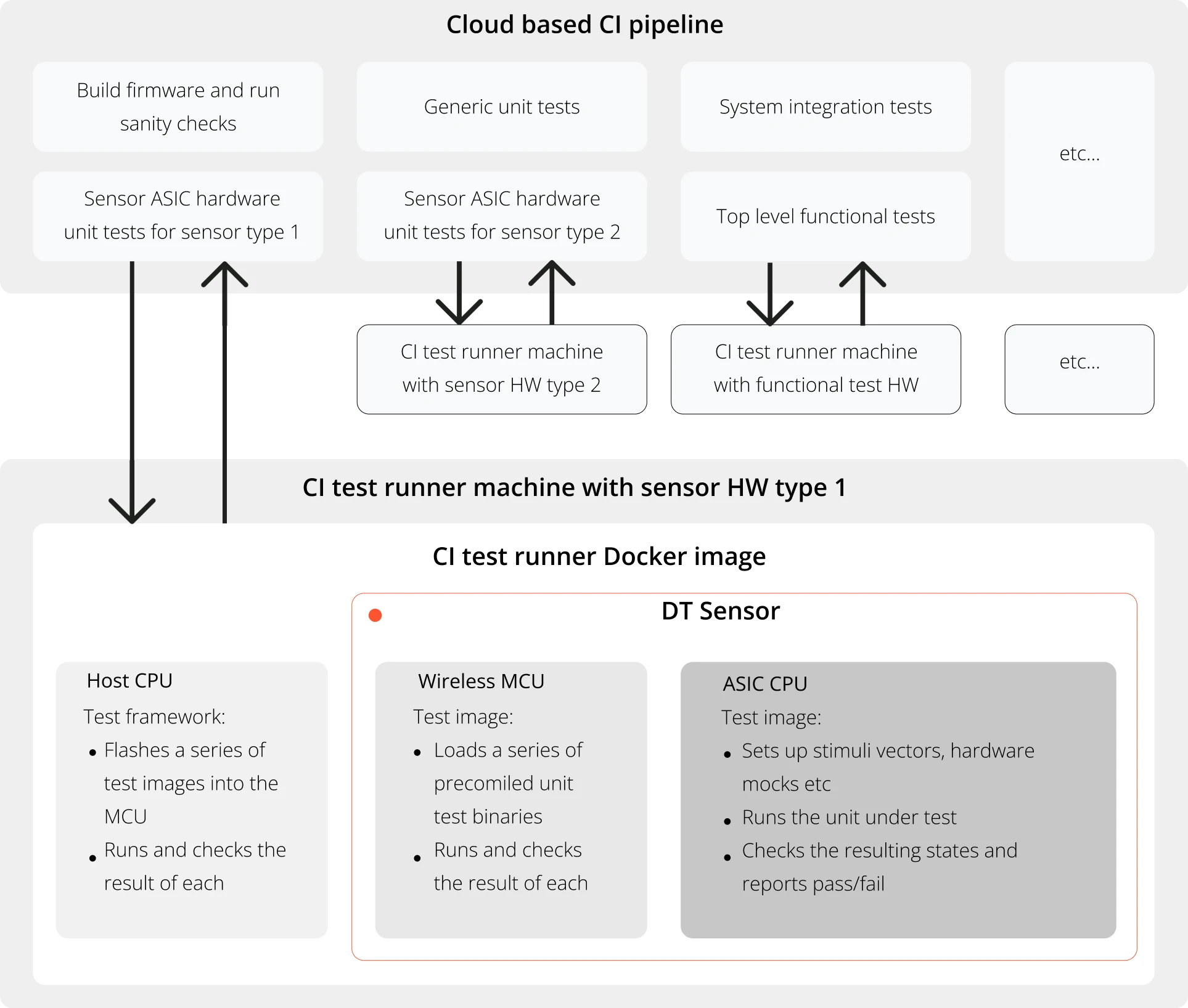
At the core of the ASIC firmware verification is a unit test framework, developed in-house specifically for the ASIC CPU. This framework allows a test to set input conditions like RAM variables, CPU registers, and flags, run the unit under test and then check relevant output states before returning pass/fail data to the wireless MCU. Input from peripherals can also be mocked where needed. The framework is lightweight enough to fit in the limited RAM, while powerful enough to make it easy to do complete testing of all logical branches and corner cases by running the test repeatedly using different stimuli.
4. Firmware Release Testing
Because long battery life is so crucial, every firmware release goes through an even more extensive set of tests than the testing performed as part of the CI process. Here, the firmware image under test is loaded onto different sensors and put through many combinations of extreme conditions over several days (and some tests even run for months): Temperatures from -40 to +85 °C, batteries that are fresh, spent halfway or nearing end-of-life, good or bad wireless communication conditions, exercising all different operating modes and functionality. The current consumption of the sensor is measured through all of this to ensure that recent firmware changes did not unexpectedly alter the expected battery life. The whole test is automated and requires only minimal human intervention.
The Result
Making the world's smallest and most power-efficient wireless sensors requires a combination of innovative hardware and firmware design, along with modern and innovative verification strategies. The end results speak for themselves: A sensor line-up with unmatched specifications and a quality that we proudly stand behind.
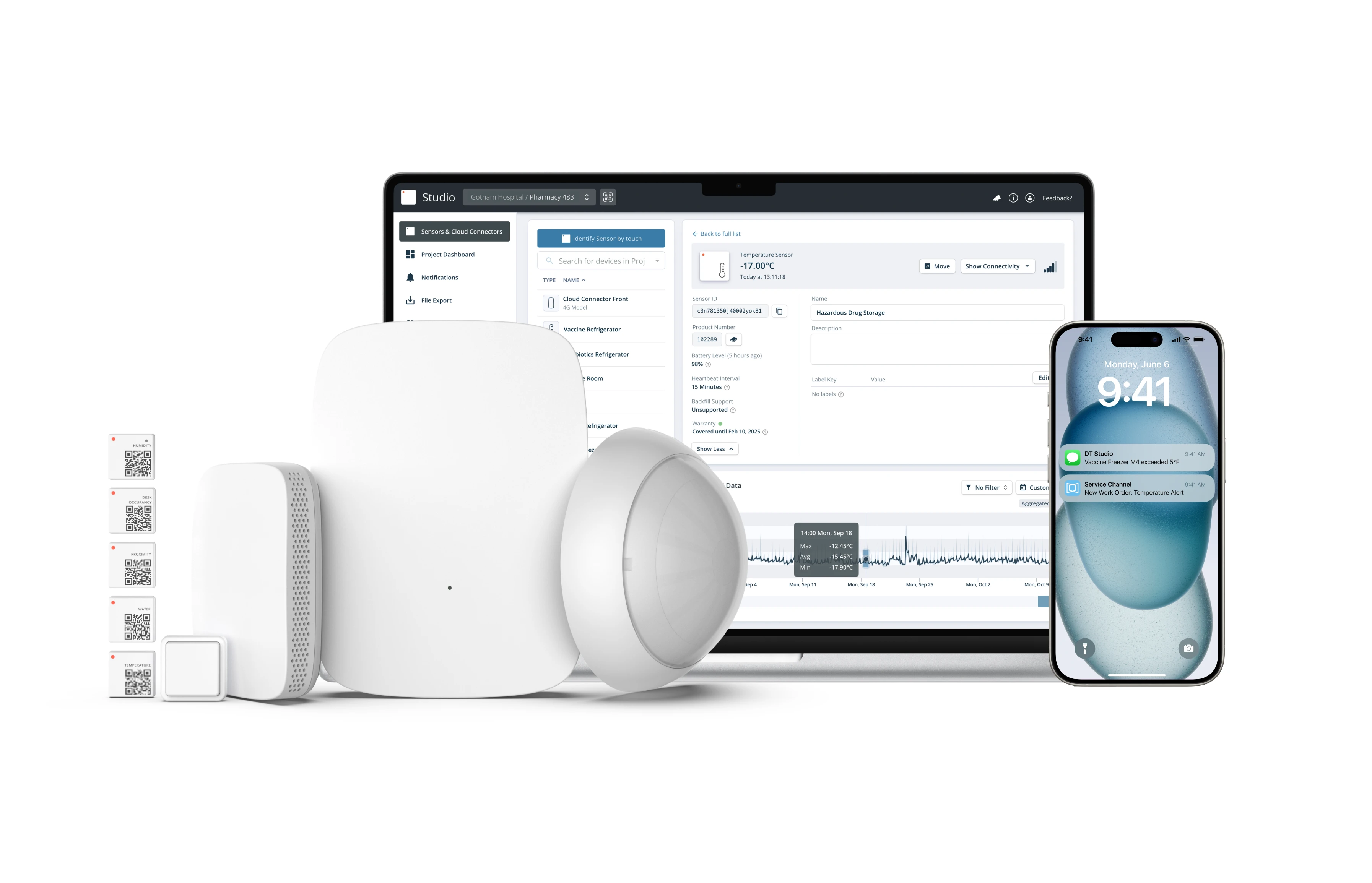
Easy-to-Deploy IoT Sensors & Infrastructure
.png)
.png)

Get Started